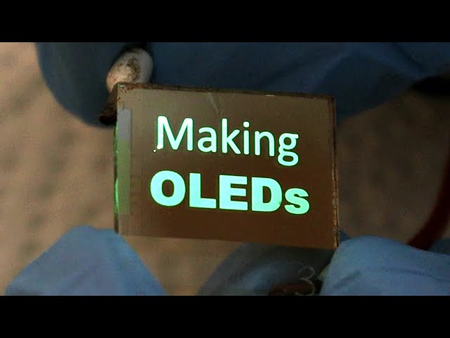
Making OLED Displays
Hey everyone. Today I want to talk about organic light-emitting diodes, or OLEDs. And the main reason to make this video is that I have sort of a personal history with OLED.
Because, in my first real job, I worked as a researcher at Philips research on Polymer LED technology. That was back in the 90s and back then, I made a lot devices in all kinds of shapes and sizes and colors. So, I guess this video is a bit of a walk down memory lane.
But it is also a test to see, if I still have what it takes to make a good OLED. In the beginning of the 1990s, OLEDs were still in the early stages of their development, and it wasn’t clear at all whether OLED as technology was going to be successful. For example, we did not know whether the life time and efficiency were sufficient for consumer products. Or whether OLEDs would be able to compete with other display technologies like for example LCD and Plasma. But OLED held a few promises, like for example the possibility to make very thin flexible displays. Mind you, back then, everybody still had a bulky CRT-based monitor on their desk.
Electroluminescence in organic materials had been known since the 1950s, but the first practical low-voltage OLEDs were actually invented by Ching Tang at KODAK in the 1980s. At the time, Tang was working on organic solar cells. And by the way, the name “organic” does not mean that the materials used, occur in nature.
It just refers to the fact that they are hydrocarbon based. Tang discovered that, in some of the organic solar cell configurations, light could be generated by running a current through them. And after patenting this invention, Tang and his coworker Steven van Slyke, published their first paper on organic LEDs. The device described in the paper consisted of a glass substrate, coated with a transparent conducting material called Indium Tin Oxide, or ITO for short. On top of the ITO, which is anode in this device, 2 very thin layers of low-molecular organic materials were deposited, the most important one being an electroluminescent layer consisting of a metal chelate called ALQ3 for short.
The device was topped off with a cathode layer, consisting of magnesium and silver. As you can see, the actual device itself is extremely thin, in total only a few hundred nanometers. When applying a voltage to the electrodes, a bright green electroluminescence could be observed from the emissive layer. As for the research that was done at Philips: we focussed on a different class of materials. Instead of using a low-molecular emitter, we looked into the possibilities of making devices of a fluorescent polymer called PPV.
These polymers are also organic but consist of long chains of this particular building block. And by modifying the side chains of the polymer, it was possible to tweak the emission color of the material over the full visible spectrum. The main reason for using polymers rather than low-molecular materials was ease of manufacturing. The OLED devices of Tang and van Slyke required several process steps involving physical vapor deposition, which is a complex and expensive manufacturing method. Basically, each one of these layers has to be evaporated in a high-vacuum and in addition requires a special shadow mask.
Polymers on the other hand can just be ink-jet printed from a solution under ambient conditions which is a more economically viable process. And it also allows for manufacture of for full-colour matrix displays rather than just monochrome displays. I worked on this project for about 5 years and when I left Philips, my colleagues gave me this clock, which contains 4 polymer LED devices. The clock itself died years ago.
But surprisingly even after 22 years, all of the LEDs still work, which is pretty amazing given the materials they are made of. Let’s have a look at the principle of the OLED. And to explain, I will use the device of Tang and van Slyke to as an example. As I have just shown, it contains AlQ3, a highly fluorescent material with a maximum emission wavelength at around 550nm.
And AlQ3 fluoresces for example under irradiation with UV-light. It absorbs the UV and then re-emits light of a longer wavelength, in this case a bright green. Here on the left, you see this effect illustrated in AlQ3 powder, and in a thin layer of the material on glass.
By the way, next to it is a blue fluorescent material in the same configurations. So, this diagram shows schematically what happens in the case of fluorescence. A molecule absorbs the energy of a photon and by doing so one, one of its electrons goes into a state of higher energy.
The excited state first loses some of its energy in the vibrational modes of the molecule, so basically this part of the energy is directly converted to heat. The remaining excitation energy can either emitted as a photon or be converted to heat by radiation-less decay. In some materials, there is also a third path which involves phosphorescence. However this path does not play a role in AlQ3. The ALQ3 molecule consists of various conjugated aromatic ring elements, which means that some of the electrons in this molecule are not bound to a particular atom, but their presence is rather distributed over the molecule. In addition, electrons can hop from one molecule to the other if their electronic orbitals have overlap.
So AlQ3 is not a good conductor, it’s not a good insulator, it’s basically a semiconductor. So, let’s say that we apply 10 volts over a layer of 100nm. This means that the electric field is 100 million volts per meter.
And at these electric field levels, even a very bad semi-conductor can be persuaded to conduct electrons. But how does this conductivity result in the generation of excited states that emit light? Well, let me try to explain in a very simplified and schematic manner. Here at the interface of the negative electrode, the molecule can be tempted to accept an additional electron from the cathode material. Especially if the cathode is made of something that easily donates an electron. Once the electron is in the material, it can start migrating in the direction of the positive electrode, due to the strong electric field in the material.
So, at this side of the device the material conducts like an N-type semiconductor At the positive electrode, an electron can be removed from the AlQ3, resulting in a positively charged molecule. Again, due to the field, the molecule is then likely to have the missing electron being donated by the next neighbor and so on, resulting in the net migration of positive charge. As you can see, this process does not involve positive ions physically migrating though the material but rather electrons that hop from a neutrally charged molecule to a molecule missing an electron. Effectively though, this is equivalent to the migration of positive charge.
So, at the ITO side, the AlQ3 behaves as a Positive-type or P-type semiconductor. And the virtual charge carrier for this conduction mechanism is generally referred to as an “electron hole” or “hole” for short. Now, even though both these conduction mechanisms involve the transfer of electrons, they are fundamentally different, because they involve different electronic states within the molecule.
And if the two electronic states meet up somewhere in the material, they can recombine, thereby creating an excited state that can release the excess energy of the electron by emitting a photon. And the excited state is basically the same thing as the state that is generated by the absorption of UV-light. Now, of course if you have equal amounts of electrons and holes injected into the material, and a 100% of them recombine, this should in theory result in a highly efficient device. But in practice, the number of holes and electrons injected will not be perfectly balanced. Let me try to explain why that is: This figure schematically shows the electronic energy levels that are involved in the electron- and hole conduction in a single layer AlQ3 device.
It is pretty complex, but in short: the energy states down here are involved in hole conduction, whereas the energy levels here participate in electron conduction. And here in an emissive material, the two charge carriers hopefully recombine. Now, on the left we have the ITO electrode that has a work function of approx.
4.6 eV, on the other side we have Magnesium with a work function of 3.6. This means that there are two energy barriers on both sides of the emitter, that have to be crossed by the charge carriers. And the thing is: these barriers have different heights: Here at the ITO interface, the energy difference is 1.2 eV for the holes and at the cathode it is only 0.6eV for electrons. And since injection scales exponentially with the energy barrier, there will be a large mismatch between electron- and hole injection. Which automatically leads to a strong decrease in quantum efficiency. So, in order to balance the N-and P-type charge, an additional layer can be added to the device that facilitates the hole transfer.
Due to its electrostatic potential levels, the layer divides the large energy barrier at the ITO into smaller steps. At the same time, it also introduces an additional energy barrier for the electrons going to the anode. And in essence, this is what improvement of OLEDs is all about: to tweak the device materials and layer structure in such a way, that energy barriers are lowered and tuned on both sides of the device to optimize efficiency.
OK enough theory, let’s just make some devices. I tried to buy PPV online, but it turned out to be very expensive, in the order of 1 euro per mg. So instead, I decided to make some devices based on AlQ3, using my recently finished thermal evaporation setup.
I wanted to make 2 types of OLEDs: a 7-segment numerical display and a display containing a fixed luminescent text. To make these, I had to do some photolithography first and I decided to use a simple resin 3D printer as the exposure tool for this. With a pixel resolution of 35 microns, it allows for easy but fairly low-resolution patterning of resist layers.
The 3D printer normally uses the LEDs of 405nm to cure the different resin layers in a 3d print. But of course, you can also use that light to expose a photoresist. Thing is, photoresists are not as sensitive as resin, and I needed about 150 seconds of exposure time to fully expose a photoresist of only 1um thick. This is also the reason why I gave the stl-files used in the 3D-printer a bit of thickness. Because thickness is basically equivalent to total exposure time.
As for the ITO-layer itself, I took the easy way here and just bought some fairly cheap glass substrates, coated with an ITO layer on Ebay. The ITO was then covered with photoresist using spin coating, after which the resist was baked for 1 minute at 100C, exposed using the 3D-printer and then developed in a dilute sodium hydroxide solution. The pattern was then etched into the ITO in about 5 minutes, using 30% hydrochloric acid. And this is the result, it looks pretty nice with the naked eye. However, if you look under a microscope, it is not all that pretty.
The edges of the ITO are quite frayed, because of the limited pixel resolution of the 3D printer and also because of the form factor of the printer pixels. But even so, this will work just fine for the experiment. On top of the ITO, an additional layer of photoresist was applied to define the active area of the devices. Because, for example in the segmented display, you don’t want to complete ITO pattern to light up, only the segments.
So, I used an addition layer of photoresist to serve as the electrical insulator. And here you see the result after development of this second layer: You can clearly see the sort of blue colored openings in the yellow photoresist layer, defining the segment- and contact areas. By the way, under a microscope, this photoresist layer has the same wavy edges of course. Next up in the process was the deposition of the organic layers using PVD, which turned out to be not quite straight forward, especially the deposition of the AlQ3. Every time I tried to evaporate it from a standard evaporation boat, it just sort of exploded and flew thought the vacuum chamber, no matter how slowly it was heated up. So eventually I found out that the boiling point of AlQ3 is much lower than its melting temperature.
And this means that you can only use sublimation for its evaporation and you need to keep the temperature well below the melting point, which is difficult with a standard evaporation boat. So, the solution I came up with here was to make a solid pill of the material and then place it on a metal grid inside a heating element. And this immediately solved the problem, because you now use very mild radiative heating to evaporate the material from the outside.
The deposition of the hole transport layer and the emissive layer could be performed during the same vacuum deposition cycle, because I have 2 thermal sources in the chamber. Here you see the two materials in the thermal sources just before the deposition. Instead of measuring the exact thicknesses of the resulting layers, I just added well defined amounts of material to the boats that would, as least theoretically, result in approximately the right layer thicknesses. Now, the last manufacturing step was the deposition of the cathode material, which had to be done in a separate run.
For one, because you don’t want to deposit the cathode everywhere on the substrate. So, before application of the cathode layer, I masked specific parts of the devices by taping narrow strips of Aluminum foil over the anode contact areas to protect them from metal deposition. As a cathode material, I decided to use Yb instead of Mg and Silver, because it only requires a single evaporation.
Yb is actually one of those rare elements that has a very low work function but is also remarkably stable to air because it forms a thin and dense protective oxide layer that stops oxidation. Yb is not expensive and easy to find on Ebay. And this is the finished segmented display, fresh from the evaporation chamber. So let me show you that these segments actually work: Here I press the negative lead against the common cathode and then, by applying a positive voltage to the ITO contacts, I can light up the segments individually. As you can see, they are quite bright and uniform at 9 V. All segments work really well, even the central segment, which only has very narrow ITO contact leads to the device.
Here is the other device, with the fixed text area. It is not perfect and has a few hot spots. But it also looks pretty acceptable for a demo.
And when I increase the operating voltage from 9V to 11 V, the brightness goes up pretty dramatically. On video, the light now looks kind of whitish, but that is not the case, this is just the camera sensor overexposing. If I bring down the shutter time of the camera a bit, you can see that the color of the LED is still the same green. Now, even after being in air for about 30 minutes, the devices still look pretty acceptable, at least with the naked eye. But if you look under a microscope, you can already see degradation setting in.
It proceeds mainly by formation of black spots, which grow gradually in time. These black spots form because oxygen and water diffuse into the device though pinholes in the cathode layer. And these pinholes are actually very difficult to avoid, unless you work in a very high-class cleanroom environment. This is because the total layer stack is less than 0.5 micron thick, so any particle larger
than that can very easily cause a pinhole in the cathode. Once oxygen and water are in the device, they will react with the freshly deposited cathode interface to form a thin non-conductive oxide layer. And this effectively creates an electric barrier on the cathode, hindering electrons from going into the material. Here is the situation after continuous operation of the device for 20 hours in air. You see that a significant part of the active device area is now black spot.
However, also notice that the area between the black spots is still at approx. emitting at the same brightness. So, the operational life time of this particular device is not limited by the intrinsic stability of the emitter material, but by the reaction of the cathode with oxygen and water. And this reactivity is actually a fundamental issue: cathode materials that allow for efficient injection of electrons, need to be able to easily release an electron themselves, which makes them an easy target for molecules with a high electron affinity, like for example oxygen and water.
And there are no materials with a very low work function that are at the same time completely stable in ambient conditions. Now earlier I showed you devices that still perform well even after 22 years of mostly shelf life. And in these devices the stability is due to a fully hermetic seal around the device. This is achieved by making the packaging exclusively from metal and glass, which both are impenetrable to water and oxygen. Unfortunately, hermetic sealing complicates manufacture of devices quite a lot, compared to when you would just use a simple glue.
Especially of course if you want to make for example a matrix display with a lot of contacts. But when we were doing research at Philips, being able to make hermetically sealed devices helped us enormously. Because it allowed us to distinguish between degradation due to running the device and due to external factors. In a sense it allowed us really focus on optimizing the intrinsic operational life of the device itself.
And once you know what is feasible as a life time, you can then go to less rigorous packaging methods which still give an acceptable shelf and operational life expectancy. After all, devices made for eternity aren’t necessarily good for business…
2021-09-04