Integrated 3D EM/Circuit Co-Simulation for First-Pass Design Win
Hello everyone, and welcome to this webinar titled Integrated 3D EM/Circuit Co-Simulation Environment for First-Pass Design Win. My name is Jack Sifri, and here is my agenda. First, I will briefly talk about the RF and Microwave industry trends, and why 3D EM is crucial and plays a big part in the overall design process. Next, I will explain to you, why did I choose this title? Then, I will introduce to you RFPro and show you a very quick demo. Number four in the agenda is the meat of
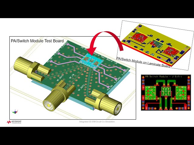
the webinar. I want to use RFPro in the design and analysis of a PA switch module, and here's a quick preview of that module. What you see here are two MMIC power amplifiers and a MMIC switch mounted on a laminate board with bond wires, and the whole laminate board is mounted onto an evaluation test board using solder bumps. Now, here's the final module with the SMA connectors, test board, solder bumps, bond wires, the laminate, and three ICs, all assembled using Smart Mount technology in ADS (Advanced Design System). At the end, I will share with you a comprehensive hands-on workshop, that is if you're interested and wanted to learn how to assemble a multi-technology structure like this using Smart Mount technology in ADS with RFPro EM simulation and analysis. Okay, let's begin with a brief talk about the RF and microwave industry trend and show why integrated 3D EM is essential. The industry trend in RF and microwave
design is driven by consumer demand for more and greater functionality, smaller size, and increasingly higher application frequency bands with broadband modulated RF signals. This directly translates into denser and denser integration of complex modules with RFICs, MMICs Passives, Packages, and antennas at higher frequencies. This also means that the design of these components and integrated modules are now becoming more challenging, because circuit simulation must definitely be combined with 3D EM simulation to account for parasitic effects of the complex multi-technology integrated structures. So, we are now at 5G with an operation
frequency in the 28 gigahertz millimeter wave band. Other high volume and high revenue applications are in the automotive radars and wireless networking at around 80 gigahertz and 60 gigahertz respectively. So, you can see the work for RF and microwave circuit designers are not getting any easier. Now, I want to explain why I chose this title for the webinar, Integrated 3D EM/Circuit Co-Simulation Environment for First-Pass Design Win. You see in the past, 3D EM simulation was performed as a separate task, disconnected from the design flow. For
example, and most of you might have experienced this flow. First the design is exported to some EM simulation tool. All SMD components and active devices are stripped off and removed from the layout and the remaining portion to be simulated must be cookie-cut out to be analyzed by the EM simulator. Now, pins are placed at every disconnected node, and the layout is then exported as a GDS file. EM simulation is run
and a large, multi-port S-parameter matrix is created to represent the EM solution without the active devices and the SMD components. This multi-port S-parameter file must then be reconnected back to the circuit with the SMD components and the active devices for the EM and circuit co-simulation in order to understand the EM circuit interaction. This reconnection process is manual, and tedious, and error prone, especially when hundreds of ports are involved. Just imagine if by error you happen to manually connect the wrong component at the wrong node, and perhaps the results were reasonably acceptable, but it is the wrong results due to this error; then the hardware will fail and it would take at least another three months to troubleshoot and rebuild. Whatever the situation is, delay to market always result in significant financial loss, and repeated hardware failures can cause the company to lose design wins repeatedly, leading to eventual closure. So, the title, "Integrated 3D EM/Circuit Co-Simulation For First-Pass Design Win", is represented by this new flow shown on the left side only. The whole
process from circuit simulation to EM analysis and EM circuit co-simulation is all integrated together and automated that designers no longer have to perform the tedious tasks in order to run EM simulation. In this new process, there is no layout modification whatsoever, and there is no manual reconnection of SMD components and active devices. The whole process and the EM setup are totally integrated, and automated, and error free. So now, let me show you this new design environment by introducing RFPro, an EM circuit co-simulation environment, tightly integrated in ADS to enable easy access to EM analysis by RF and microwave circuit designers, whenever they need it during design. RFPro addresses three common requests: Number one: No layout modification or cookie cutting to do EM analysis.
You no longer need to strip off and remove components. All this is automatically done by RFPro. Number two: Automatic and correct setup of EM analysis to produce results that can be trusted with confidence. Yes, RFPro has intelligence to automatically create for you correct EM setup. And, number three: is tight integration with circuit design
simulators in ADS and Cadence Virtuoso with the same environment to access FEM or Momentum EM solvers. To see RFPro in action, please allow me to start by showing a demo to introduce RFPro to you, and especially to those of you who haven't seen RFPro yet. It's a very quick demo that shows how quickly and automatically I can set up an EM circuit co-simulation without any manual reconnection errors.
Here we go: In this short demo I would like to show you how to quickly setup and EM simulate your design with RFPro. From the layout page, RFPro is launched from the Tools menu. RFPro automatically assembles the entire design, including its pins and components.
Components with circuit models, like FETs and SMT devices are usually represented with circuit models and do not require EM simulation. So, by dragging the components down in the analysis section allows RFPro to combine and co-simulate these circuit models with the EM simulation results of the layout. Similarly, by dragging all the design pins down in the analysis section allows RFPro to automatically create a port for each pin, with a reference ground that is closest to the pin. Here in the Option tab, I set the
simulation frequencies, and I select the EM simulator. In this case I chose the Momentum microwave engine. Next, I run the simulation. And once it's done, I can immediately view the results such as S-parameters of the EM simulation. I can also create test benches for ADS that automatically combine the EM co-simulation results of the circuit models with the EM simulation results on the layout. So, in ADS, I open the top level schematic page, and from there I can shift views and simulate both, my original circuit level design with circuit models as shown here, or I can shift the view to the EM model from RFPro and simulate it, and see how my simulation results have changed.
I can even keep the simulation results in the memory by turning the History on and be able to display both results on the same plot for better viewing of the change in the results from both views, circuit versus EM, as shown here. And this is all there is to it. Okay, let's move now to item 4 in the agenda. I want to illustrate to you how this whole integrated and automated design flow is used in the design and analysis of this complex PA / Switch module assembly. In this example, I have two MMIC power amplifiers and a MMIC switch, all assembled on a laminate board and connected with bond wires as shown here. This laminate board module is then
placed and assembled on another test evaluation board. Notice I decided to mount the laminate board using 3D solder balls components, and I have also used bond wires as well, just for the purpose of illustrating to you the richness of mixed multi-technologies assembly and simulation in ADS, and to show you how all these mixed technologies can be automatically and easily co-simulated, circuit and EM together without having to touch or modify any layouts. It is all automated. I have also imported and used 3D SMA connectors from
EMPro and placed them at the output of the test board as shown here. What you see is the test board, the laminate board, the three MMIC ICs, bond wires, solder balls, and connectors; and this is what I will be showing you in the next segment of my talk. I was browsing the Internet and I saw this Triquent or Qorvo now Quad-band power amplifier module that is used in handsets and on the Ipad 3 board as shown here. I looked up the functional block diagram and notice it is similar to what I'm showing today, namely 2 PA ICs switched by some control circuit; and similarly this Amalfi PA front-end module is mounted on an evaluation test board, just like the example I have constructed for this webinar. Now, let me go over the whole design process and show you how to conveniently assemble this complex, multi-technology PA Switch module using drag-and-drop Smart Mount capability in ADS, and simulate it with RFPro. Please pay
attention to how quickly I can set up and run EM circuit co-simulation without any manual reconnection errors. Now, to build this whole multi-technology project, first I started a new workspace in ADS, and I called it MCM Workspace. Next, I wanted to bring in all design libraries into this workspace. To do this, I clicked on the DesignKits tab and opened the Manage Libraries window. Now, here you can see I have imported all the libraries that I needed to build up my whole module; for example, you can see the SPDT switch library, the LTE MMIC PA library the 3D solder bumps components and SMA connectors imported from EMPro. And importing these libraries is
simple; just click on Add Library Definition File and browse to the library and bring in the lib.def file as shown here on all the imported libraries. OK, let's now look inside each folder. Folder one contains the MMIC PA it is the same PA you saw earlier in the video demo, I just wanted to share more useful information with you. First, since I will be placing this MMIC onto a laminate board of different technology, I will need to specify this multi-technology assembly in the Options > Technology > Nested Technology page. Notice I have checked the box
to allow me to use smart mount in order to mix this MMIC PA technology with another technology, namely the laminate board technology. I have also selected bottom mount for the type of mounting, not flip chip, bottom mount. By applying smart mount here, ADS automatically and behind the scenes does the scaling and layer mapping between the two technologies. Now, for those of you who have used the traditional nested technology method, you no longer need to go through the setup anymore. Smart Mount automates the process and does the scaling and layer mapping for you behind the scenes. Now, here's a quick review on RFPro. From the layout page RFPro is launched from the Tools menu.
Notice all components with the layout view will be EM simulated. Components with a schematic view will be co-simulated with the EM. In other words, all circuit models or S-parameter models will automatically combine with the EM results, and this by itself eliminates any manual reconnection errors. Now, dragging the pins down in the analysis section automatically creates ports with a reference ground closest to the pin. Circuit model components are brought
down in the analysis section in order to automatically combine them and co-simulate them with the EM results. Clicking on Options allows you to set the simulation frequency and simulation type; so we run the simulation, and once it is done, you can view S-parameter results and create a test bench for ADS. Now, we open the top level test bench in ADS, and first, let me select the original circuit design schematic and simulate it as a reference. Let me turn the History on to keep the result saved on the plot. Next, I switch to the EM model from RFPro and the view has the EM model which is the S-parameters matrix and the FET models which are already and automatically connected to the correct pins.
We click Simulate and we can see the difference in the results; EM versus original circuit level design results. Next, let's move on to the MMIC switch in folder two. Here is the layout view of the switch with one input port and two output ports, along with two control pins to activate which side of the switch is on or off by applying either plus or minus 3 volts. Again, I launch RFPro from the Tools menu. The whole design is exported to the RFPro page; and similar to what I did on the PA, I drag down the pins to form the ports, and I drag down the circuit components models to be co-simulated with the EM results of the layout.
Then, from the Options tab, I set the simulation frequencies and the simulation type, and I run the simulation. Once the simulation is completed, we can view the S-parameters results and we can create an EM model in ADS. So, in ADS we can use this model in a test bench to see the switch EM simulation results. Now here, in the test bench, I selected first the original schematic view and you can push into the symbol and see the content of the switch sub-circuits. Or, we can shift views and select the EM model view that we have just finished simulating in RFPro. If you push into the symbol now, you see
the EM model S-parameter blocks with all the FETs, automatically connected to the right port without any errors. You see, there is no possibility of making any manual connection errors, all connections are done automatically by RFPro. So here, I use plus three volts on one side control gate pin and minus three volts on the other arm. I then simulate and see the response of the switch and isolation. Next, I switch the plus and minus 3 volts to test the other arm of the switch and I simulate. So here, you can see now the red curve is on top and the blue on the bottom. So, the switch is working fine as
designed and as expected. Okay, now let's move to the next level of assembly in folder three. As you see, I have dragged and dropped the three ICs onto a laminate board. The scaling and layer mapping of the two technologies, the MMIC and the board technologies, are done automatically with smart mount.
This is the layout of the module with the laminate board and three ICs, assembled face up onto the pc2 layer. This is the substrate. Notice I had to cut a hole or a well in the top dielectric layer in order to insert and place all three ICs onto the pc2 layer. And this is how I made the holes or the wells into the substrate. I just draw a rectangle cut in the dielectric layer and I select all the shapes in that dielectric layer and then I use the Merge > Union Minus Intersection command to create that cut.
And here's the 3D view that shows the cut and the assembly. Now, some of you might ask, How does ADS know where and what layer to place the ICs, the vertical position in the substrate? You see, once you drag and drop the ICs into place using smart mount, I right-click my mouse on each of the ICs and I can select the mounting layer as shown here. And here you can see I chose the mounting layer pc2. Now, here's the 3D view of the module. Now, notice as I rotate the module, notice the connecting pads at the bottom of the module that are cut with clearance around them. These were made in order to connect to another test board later on with solder bumps. As we did before, I launch RFPro from
the Tools menu. So, let's now EM circuit co-simulate this whole smart mount PA switch module. The whole layout is brought in here. You can see all components including the MMIC FET devices that have schematic symbols and circuit models that will be automatically combined with the final EM results of the whole module. All pins are also included here, signal and ground pins. So, we drag the pins and the components down in the analysis section, just like we did for the ICs. Ports will be created and they have two pins positive and negative. The negative pin of the port is the ground return
pin you have decided to use in your layout; and here are the FET circuit model components that will be co-simulated at the end with the EM results. Next, like what I had shown before, the Options menu allows you to set up the simulation frequency and the type of simulation. Of course I have chosen the FEM simulation here. Next, I run the simulation, and at the end, I go ahead and generate that EM model to use in ADS to plot the results.
So, in ADS, I open the top level test bench, and just like I showed earlier, you can select the EM model view as shown here. And if you push into that symbol now you can see the model that came from RFPro. It has the complete S-parameter matrix along with all the FET devices automatically connected. So, there is no chance for any manual connection errors. Okay, so let's simulate this and see the response; and here is the response of the PA/ Switch laminate level results. S31 is blue on top with S21 on the bottom it's the
isolation. Now, if we change the voltages to change the switch arms, plus and minus three, and simulate, so now we can plot the other arm switched module, as shown here. A better way to interpret the results is to overlay the MMIC PA standalone EM results we had previously gotten.
So, here I am superimposing the PA results standalone shown in pink and you can see that the module results acquired some loss. It resulted in lower gain and also shifted downward in frequency due to the bond wires and other parasitic effects. One thing I want you to pay attention to is this low frequency blip that is popping up outside the band. What is it? I want to make sure I understand it before shipping the design and I will come back to it later. Okay, now I want to move to folder 4 where the laminate board module is placed on top of another evaluation test board with solder balls. But first, let me open the laminate board module in folder 3. And I wanted to set it up with smart
mount, so I opened the laminate layout, here it is, and I click on Options > Technology > Nested Technology, and I check the smart mount box like we did before. That is all I do. ADS automatically configures the technology layer mapping and scaling if required; it is all done behind the scene without having the user to do anything else. Now, let's open the test board layout in folder 4. As mentioned earlier the laminate board sits on the test board with solder bumps connection.
The laminate board signal lines go down through vias to the bottom side to connect to the test board with solder bumps. Let me show you. Let's push down on the laminate board and turn it around to show you the solder ball connection pads with clearance away from the ground plane. These pads will have solder balls connection to the test board.
Now, I would like to construct good 50 ohm lines on this test board to connect to the laminate board lines. Very conveniently, I took advantage of an integrated and built-in tool in the layout called "Controlled Impedance Line Designer" (CILD) which quickly and easily allows me to analyze any microstrip, strip line, or coplanar lines. Look here, it even automatically loads in and uses the substrate stack of your current design; or you can change it to another substrate if you wish.
So, I use the coplanar structure for my board where the signal path is on the pc2 layer, and the ground is on the bottom pc3 layer. Now, here's a line with the width of 0.3 millimeter and clearance of 0.1 millimeter, and when I simulate it it yielded 45
ohms. Now, reducing this line width to 0.1 millimeter and simulate, it yields 58 ohms. Finally, after few adjustments I got a line width of 0.2 millimeter with clearance of 0.1 millimeter and that gave me a good 50 ohm line with attenuation of 0.0026 db
per millimeter. And this is what I have used for my lines, as shown here on the layout. I routed these 0.2 millimeter lines on the pc2 layer and I specified a 0.1 millimeter clearance on the coplanar ground plane, as shown here. You see, I constructed that ground plane, and once I have the ground plane, I double-click on it, and you can see the clearance is 0.1
millimeter on the top. Later, I will show you how I can verify this good 50 ohm line impedance using RFPro's user-defined analysis which focuses and runs EM analysis only on one part of the structure, namely the RF lines here. Now, do you remember at the beginning, I had showed you how I imported all of the design libraries into this workspace. I clicked on Manage Libraries, and I brought up all the libraries I needed, and now here you see the 3DEM components that I have brought in from EMPro, namely the solder bumps and the 3D connectors. Now, in the main window of my workspace, I do see these solder bumps and now I can drag its footprints into my layout and specify the layer they sit on. So here, you can see I have used them to sit on
the pc2 layer, and I place them under the pads on the bottom side of the laminate board, as shown here. Next, I open RFPro and utilize the "User Defined Analysis" to simulate and check if these .2 millimeter coplanar lines are truly 50 ohms. User-Defined Analysis allows you to select any part of the design and analyze it. Simply bring down the nets that you
want to analyze and RFPro solves it. So here, I took advantage of the virtual pins feature in RFPro and I inserted virtual pins at the end of the line, close to the solder bump where the laminate board signal meets the test board signal line. These new virtual pins are not in the original layout. RFPro allows me to create them anywhere and at any layer. So here, you see my line starts with the
input port and ends at the end where the solder bump is. To create a virtual pin, you just right- click the mouse and select "Create virtual pin", then click the mouse at the correct location and choose the corresponding layer. So, I went ahead and analyzed this RF line and I confirmed that it is indeed a good 50 ohm line. The return loss is better than 20 db, and the insertion loss is less than 0.1
db at the highest frequency. And also here, I plotted the impedance and it shows it is around 50 ohms and that is what I wanted to verify. Now, let me simulate the whole multi-technology structure including the board, the laminate, the solder bumps, the bond wires and the three MMICs. Please keep in mind I'm mixing different technologies here and different dimensions including microns for the MMICs and larger millimeter units on the laminate and test board. You see, RFPro is capable to handle this mix of technologies. So, I open RFPro, just like we did before. and I analyze now the whole board, and truly this is the beauty of this integrated 3DEM co-simulation environment; everything is automatically imported from layout to the RFPro page.
You do not touch the layout. You run the EM simulation with automatic circuit models co-simulation, and if you wish, you can add virtual pins on the RFPro page and do customized user-defined analysis. It's very flexible and automated. Just like we did before on the laminate board, I drag the pins and circuit components down in the analysis section, and I'm ready to proceed with my FEM simulation. Here I set up the frequencies and the type of simulation, namely FEM here, and I'm ready to run my simulation. So here, I went ahead and ran the
simulation; and once it was completed, just as we did before, I went ahead and created an EM model to use an ADS. And here in ADS, I open the top-level test bench for the whole module, and here is the EM model from RFPro which has the complete S-parameters matrix, all automatically connected to the active FET devices. So, I go ahead and launch the simulation. Notice the Expression Manager at the right side of the Data Display in ADS 2021 Update 1.0. It contains all of the parameters that can be plotted, and all you have to do is to drag-and- drop whatever you want and the plot is automatically created for you. And you can do all the editing with the right-click of the mouse. I thought I'd share these new and cool features with you. So, here is the response of the whole
module, simulated in RFPro with FEM. Let me let me now overlay the two responses we simulated earlier, on the laminate board, and on the MMIC PA standalone. And here they are. Again, notice the huge spikes showing up around 350 megahertz, it is lower in magnitude on the laminate board, and much lower at the MMIC PA level. As we will see later, the bond wire from the PA to the laminate contributes to this spike. You will see later, I will even verify it to you by just adding 0.8 nano Henry inductor at the drain DC bias line on the MMIC PA alone to replicate the effect of the bond wire. And now, with added solder bumps and bias lines included, it resulted in an
even larger effect and increased the size of that spike. So, one clue we are getting out of this is the DC bias at the drain needs to be better isolated from RF at the PA level. But since this spike slightly shows up at the PA standalone level, this enticed me to take advantage of the new Winslow probes in ADS 2021 and use them to perform stability analysis on the PA and on the whole assembly. I borrowed this slide from my colleague, Matt Ozalas, who has done a lot of work on this new Winslow probe for stability analysis. In fact, I have included in the resources reference materials and videos on that topic from Matt. The Winslow probe is a general stability probe in
the simulation tool. This probe can allow you to apply just about any type of stability analysis technique to your circuit in a very straightforward manner. This probe is nicknamed the Winslow probe because it was developed by Tom Winslow from MACOM.
Tom has developed this probe and worked with Keysight to get it into our tools. The top right portion of this slide outlines all different methods that have been developed on stability analysis. The bottom portion of the slide displays the stability analysis results from this new Winslow probe versus many of the other popular methods. You can see the probe can be applied to all other methods and the results perfectly matches them all. So, I went ahead and used the probe on my
design to study that low frequency stability issue. I decided to focus only on the MMIC PA, since it is the source of that low frequency spike. So, first I used the original schematic design with the probes and here are the results.
You see here, the Kurokawa function inverts the driving point impedance into admittance, and then displays the frequencies where right-hand poles or oscillation is being detected. The spike is hardly seen, but the Winslow stability probe detected at 374 megahertz instability at the drain of the output FET. So next, I added the 0.8 nano Henry at the drain bias pad. Notice the spike got higher and the Winslow probe detected instability at both gate and drain. Please note that the second stage has an LRC feedback loop between the drain and the gate as shown here, specifically created to stabilize the device and flatten the response at the pass band. You see, the PA was originally designed for unconditional stability, the FET structures were unconditionally stabilized before even creating the matching networks, the input, interstage, and the output. So, there must be something more I need
to know and investigate further. Now here, I repeated the simulation with the EM model from RFPro and with the 0.8 nano Henry inductor to represent the bond wire. The result shows and confirms that the unstable frequencies occur around the output FET through the feedback loop at the drain and the gate of the output FET, around 340 megahertz. Now, I want to utilize RFPro near field plots to look at the current densities at various frequencies, to understand more about this dilemna. This is called circuit excitation with
EM. You basically drive the designs EM model with circuit simulation stimulus and view the results in RFPro. let me show you how. First, I drive my circuit with an AC source. Here I'm applying a 1 volt AC analysis swept from 0 to 10 gigahertz. I even went further and I swept the AC source for you, just to show you how it shows up in RFPro.
Okay, here I labeled my data set and data display with a different name, by adding the extension under score AC for AC simulation. In RFPro, under the Results tab, I click on the "Near Field Results" and I ask for the "Current Density" and I select "Circuit Excitation" option. Now, for the circuit excitation option, I browse and select the AC circuit simulation I have just performed with the data set name that has the underscore AC extension. The Circuit Excitation window displays the selected data set as shown here; and next I select what frequency I want to display the current densities at, as shown here. So, here's a sample at 330, 350, 380, 400, and 1000 megahertz respectively. This is the current density at 330 megahertz, just slightly below the frequency of the spike we saw.
The big choke inductor have narrow lines is doing its job blocking the RF out from the DC lines. But, I do see cross coupling between the gate DC line and the drain DC line on the top - and this needs to be better isolated by separating them further. Now here, we up the frequency to 350 megahertz, and now we clearly see the effect of the blip or the spike. Also,
notice; look at the coupled current density at the FET top Via. Now, we go up to 380 megahertz and we still see the effect of the blip, but a bit lower than that at 350 megahertz. Now this one is at 400 megahertz, and we see the current density at the drain line is going lower and here at 700 megahertz, the effect of the spike or blip is gone.
Next, we start moving towards the low edge of the pass band where the PA start accumulating gain and RF output power. So, this is taken at 1 gigahertz. Now, this one is at 2 gigahertz, where the PA has lots of RF power delivered to the output, and we do see the output matching network RF current density high at the output matching network inductors. But, I still see some high current density leakage at the top DC bias area which needs to be improved and have better isolation from the RF section.
So, you see this circuit excitation and current densities plots give you a lot of insights to your design and help investigate troubled issues, like stability and coupling effects. So, on this low frequency stability issue, I had a nice discussion with my colleague Matt Ozalas about it. He got interested and did some preliminary investigation on it and without going into details his analysis states that a combination of gate and drain loading on the output device might be causing the instability. In other words, the problem could be related to a transistor level instability that happens for a specific loading condition, which the circuit happens to stimulate at that low frequencies. It just happened that the loading at the gate around 330 megahertz moved to an open on the Smith Chart, and this could have been a result of the FET model used from the demo kit which I used in this design. Now, before I close, I just wanted to show you here how you can also sweep the magnitude of the AC source in RFPro and see the results accordingly.
This is the current density taken at 1 gigahertz with an AC source at 0.1 volts. Next, we move it to 0.4 volts; then we move it to 0.7 volts; and finally to 1 volt. You see, this sweep feature could similarly be applied to vary for example the source input power to a power amplifier and check its response under larger signal with Harmonic Balance. Or, you could use it to sweep, for example, the phase angle of a phase shifter interfacing a beam steer antenna, and be able to look at the far field and scan the beam of the antenna as a function of this swept phase angle. I do have a 5G demo application example on this if you are interested, and it is included in the resources.
OK, let me wrap up now with some final results I wanted to share with you. Here is the SMA connector I imported, and here I simulated it in RFPro. The return loss is better than 17 db at the highest frequency with 0.1 db loss. Now here, I added the connectors to my module and performed another User-Defined Analysis on the RF line starting from the connector and ending just before entering the laminate board at the solder bump junction. In this view, you can even see the virtual pins I have added at the laminate side to use in the User-Defined Analysis; and notice, the RF line here has very good return loss, and very low loss.
Okay, here are the overall simulation results on the whole module. You can see there are few issues that need to be looked at and improved, here are a few of them: Number one, the PA standalone, if you remember, has 27 db of gain. At the laminate assembly level, we lost three and a half db, and we lost another two and a half db at the test board assembly level. This 6 db of loss seems large, and I'm sure big part of it can be recovered by revisiting critical junctions in the assembly and reduce the mismatch losses. Number two: the low frequency spike we talked about needs to be better understood and fixed. Also, the bias network needs to be
improved and have better isolation from the RF section. Number three: We need to address the coupling issues we extracted from the "Circuit Excitation Current Density" plots, if you remember. And number four: we have to sub- analyze and improve on the whole module return loss, S11 and S22 as shown above. It should be better than two to one VSWR or better than -14 dB. Now quickly, I want to mention some good information on the bond wires and solder bumps in ADS 2021 and the latest ADS 2021 Update1.0. You see in ADS 2021, and that is what I have used here in this webinar, the bond wires were placed from the ADS layout page by using the Insert Bond Wire pull-down menu in the layout page, as shown here.
Also in this webinar, I have imported the solder bumps library from EMPro using the Manage Libraries window, as I have shown earlier. I was able to use the solder bump footprint and drag it into my layout. But now, in ADS 2021 Update 1.0, you can also do this directly from the RFPro page.
You see in RFPro, just right-click the mouse and a new menu pops up that says "Create new bond wire" or "Create new solder bump". For bond wire, you just click at the begin and end position to display a wire bond. Here you can see I just clicked between the pink interconnect lines and created this bond wire just for illustration - and the same thing with the solder bump; once you say Create New Solder Bump, a new window opens up and it has all the editable parameters to define and use the solder bump you want you want as shown here. So, all of these new features are in ADS
2021 Update 1.0 and I thought I'd mention it to you. Okay, so this brings us to the end of this webinar. Now, some of you might want to learn more about what I showed today; how to assemble multi-technologies together using smart mount and simulate it with RFPro. Therefore, I have created this comprehensive hands-on workshop for you to help you master the process. It is a do-it-yourself workshop that has detailed step-by-step instructions.
So, this takes us to the end of this webinar. In summary, what I have presented to you was a demo I put together using a demo design kit so that I can show you how you can take full advantage of this error-free integrated 3DEM co-simulation environment in ADS. I really hope it was useful and I hope all these integrated analysis tools I have presented would be useful to you and help you to iteratively troubleshoot design issues as you are in the design phase to help you discover the problem areas in your designs and get you to produce first pass designs win. So, I thank you very much for attending this webinar.
2021-01-31